This site uses cookies to improve your experience. To help us insure we adhere to various privacy regulations, please select your country/region of residence. If you do not select a country, we will assume you are from the United States. Select your Cookie Settings or view our Privacy Policy and Terms of Use.
Cookie Settings
Cookies and similar technologies are used on this website for proper function of the website, for tracking performance analytics and for marketing purposes. We and some of our third-party providers may use cookie data for various purposes. Please review the cookie settings below and choose your preference.
Used for the proper function of the website
Used for monitoring website traffic and interactions
Cookie Settings
Cookies and similar technologies are used on this website for proper function of the website, for tracking performance analytics and for marketing purposes. We and some of our third-party providers may use cookie data for various purposes. Please review the cookie settings below and choose your preference.
Strictly Necessary: Used for the proper function of the website
Performance/Analytics: Used for monitoring website traffic and interactions
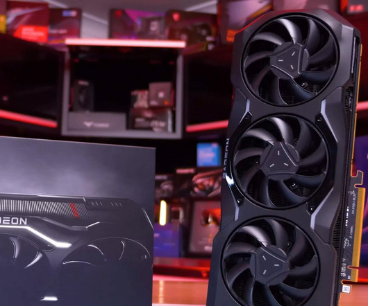
The December 2022 patent describes a GPU design split across multiple GPU chiplet sets. Each chiplet has a frontend die paired with several other shader-engine dies. The clever part is that these GPU chiplets can flexibly combine in various configurations.
Recently, users have struggled with stability issues related to Intel's Core i9-14900K & 13900K CPUs. Those with the processors have noticed increased game crashing, leading numerous developers to issue support notices. Intel said it would investigate.
In a note to investors this week, Bank of America said, "Consider it a top AI pick." It wasn't talking about Nvidia, even though BofA considers Green Team the undisputed winner of the GPU wars. It was referring to Broadcom, which recently announced a 10-to-1 stock split and better-than-expected revenue.
This minuscule chip packs 256GB of storage into a single die using WD's cutting-edge 8th-generation BiCS 3D NAND tech developed jointly with partner Kioxia. The manufacturing technology enables WD to fit 218 layers in a single die, almost twice the 112 layers most NAND flash memory today comes with. By.
Speaker: Tim Sarrantonio, Director of Corporate Brand
Do you really know your donors? Not just what they give, but who they are? 👥 In this interactive session, we’ll break down how nonprofits can use behavioral indicators (affinity, recency, frequency, and monetary value) to build prospecting segments that go beyond wealth screening and actually align with donor identity. You’ll walk away with practical strategies to move beyond basic demographics and cultivate supporters based on how they already engage with you!
First up, Samsung took the wraps off two new process nodes aimed at pushing the limits of chip performance and efficiency. The headliner is the 2nm SF2Z process, slated for mass production in 2027. This one packs a clever trick with a backside power delivery network (BSPDN) that routes the.
We organize all of the trending information in your field so you don't have to. Join 12,000+ users and stay up to date on the latest articles your peers are reading.
You know about us, now we want to get to know you!
Let's personalize your content
Let's get even more personalized
We recognize your account from another site in our network, please click 'Send Email' below to continue with verifying your account and setting a password.


Let's personalize your content